NON-CESIATED SOLID STATE ELECTRON EMITTERS (COLD CATHODES) & THEIR APPLICATIONS IN VACUUM MICROELECTRONICS
INTERIM PROGRESS REPORT
Professor Umesh K. Mishra
Robert D. Underwood
December 31, 1997
U.S. ARMY RESEARCH OFFICE
DAAH04-95-1-0157
UNIVERSITY OF CALIFORNIA, SANTA BARBARA
Department of Electrical & Computer Engineering
APPROVED FOR PUBLIC RELEASE;
DISTRIBUTION UNLIMITED.
THE VIEWS, OPINIONS, AND/OR FINDINGS CONTAINED IN THIS REPORT ARE THOSE OF THE AUTHOR(S) AND SHOULD NOT BE CONSTRUED AS AN OFFICIAL DEPARTMENT OF THE ARMY POSITION, POLICY, OR DECISION, UNLESS SO DESIGNATED BY OTHER DOCUMENTATION.
List of Manuscripts
·
D. Kapolnek, R. D. Underwood, B. P. Keller, S. Keller,
S. P. DenBaars, and U. K. Mishra, “Selective area epitaxy of GaN for
electron field emission devices,” J. Crystal
Growth, vol. 170, pp. 340-343, 1997.
·
R. D. Underwood, D. Kapolnek, B. P. Keller, S. Keller,
S. P. DenBaars, and U. K. Mishra, “Selective-area Regrowth of GaN
Field Emission Tips,” Solid-St. Electron.,
vol. 41, pp. 243-245, 1997.
·
R. D. Underwood, D. Kapolnek, S. Keller, B. P. Keller,
S. P. DenBaars, and U. K. Mishra, “GaN FEA diode with integrated
anode,” in Technical Digest of the 10th
IVMC. Seoul: EDIRAK, 1997, pp. 132-136. [also submitted to Journal of
Vacuum Science and Technology B]
· R. D. Underwood, D. Kapolnek, B. P. Keller, S. Keller, S. P. DenBaars, and U. K. Mishra, “Selective-Area Regrowth of GaN Field Emission Tips,” in Proceedings of the Topical Workshop on III-V Nitrides (TWN'95), I. Akasaki and K. Onabe, Eds. Nagoya: Pergamon, 1997, pp. 181-183.
(1) Scientific Personnel
·
Professors
Umesh K. Mishra and Steven P. DenBaars.
·
Post-doctoral
researcher Stacia Keller.
· Graduate Students Robert Underwood, David Kapolnek, and Peter Kozodoy.
(3) Inventions
· Submitted patent disclosure on InGaN-Coated Field Emitters.
(4) Scientific Progress and Accomplishments
Nitride-based semiconductors
are showing great promise in the area of cold cathode emitters. Cold cathodes based on GaN diodes with low
work function coatings[1] and planar AlN emitters have been recently
reported[2-4]. The primary limitation
of the above mentioned devices is their low efficiency. GaN can also be selectively grown to form
pyramidal structures that may be used as field emitters in field emitter
arrays(FEAs). FEAs will have potentially
higher efficiency if operating voltage can be lowered sufficiently. The growth of GaN has been optimized in
previous work of this program. Work
over the past year has concentrated on fabrication of various device structures
for evaluating the effectiveness of GaN for field emission. Fabrication of the following device types has
been achieved in the past year:
·
GaN
field emitter array diodes with integrated anode
·
Gated
field emitter arrays
·
Diamond
coated field emitter arrays
·
InGaN/GaN
field emitter array diodes with integrated anode.
Each of these device types
will be discussed in turn in terms of design, fabrication, and available
measurements.
Lowering the Operating Voltage by Device Structure
In
our previous work, we fabricated GaN field emitters with no other structures
and used an external anode to measure the emission current. This approach has several problems. First, it was difficult to determine the
anode-cathode separation. This
distance is a critical parameter for field emitters as the emission is
determined strongly by the field at the tip surface. Secondly, only large separations (~0.5 mm) were possible with
this method. Thus, high voltages were
necessary in order to achieve field emission[5]. The high voltages made the arrays susceptible to damaging arcs
that tended to destroy the cathodes.
One method of lowering the operating voltage is by bringing the
extracting electrode (positively biased with respect to the tips) closer to the
top of the pyramids. One common method
in vacuum microelectronic field emitter is to add a gate structure[6]. Another method is to fabricate an anode
on-wafer and control the spacing using microelectronic processing methods. Devices of both types have been fabricated
and will be discussed below.
GaN Field Emitter Array Diode with Integrated Anode
 GaN FEAs with integrated anodes are useful devices for determining the
usefulness of an emitter material for field emission. Emitter material effects FEA device operation mainly through its
work function and reaction with the residual vacuum gases. A low work function provides lower operating
voltage and an inert surface should provide stable emission. Another advantage of our structure is that
it has an extremely simple fabrication process flow. There are no critical alignments and the anode-cathode spacing is
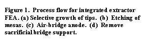
determined quite simply by a resist layer thickness. Figure 1 shows the processing steps involved. First, the GaN pyramids tips are grown
selectively using a SiO2 masking layer. Then, mesas are etched to isolate the devices. Next, an air-bridge process defines the
anode over the cathode tips. Finally,
the air-bridge support sacrificial photoresist is etched from under the bridge
to leave a freestanding structure. An
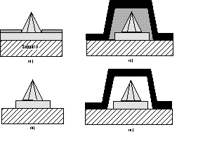
SEM of a completed device is shown in Figure 2.
GaN FEAs with integrated anodes are useful devices for determining the
usefulness of an emitter material for field emission. Emitter material effects FEA device operation mainly through its
work function and reaction with the residual vacuum gases. A low work function provides lower operating
voltage and an inert surface should provide stable emission. Another advantage of our structure is that
it has an extremely simple fabrication process flow. There are no critical alignments and the anode-cathode spacing is
determined quite simply by a resist layer thickness. Figure 1 shows the processing steps involved. First, the GaN pyramids tips are grown
selectively using a SiO2 masking layer. Then, mesas are etched to isolate the devices. Next, an air-bridge process defines the
anode over the cathode tips. Finally,
the air-bridge support sacrificial photoresist is etched from under the bridge
to leave a freestanding structure. An
SEM of a completed device is shown in Figure 2.
Figure 2. SEM
of completed FEA diode with integrated extractor. Figure 2. SEM of completed FEA diode with integrated
extractor. 
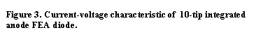
The
first measurements of these devices produced emission at substantially reduced
voltages compared to the external anode devices. Emission in the microampere range was achieved by a 10-tip array
at only 500 V at an anode to cathode separation of about 2 mm as shown in Figure 3. The voltage is about half of the turn-on
voltage achieved by the external anode arrays.
An aspect that is very encouraging is that the measured device had
rounded pyramid tips. Thus, tips with
sharper profiles should emit at an even lower applied voltage. Sharper tip arrays have been fabricated but
not measured as of yet.
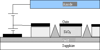
Gated GaN FEAs

The diode structure is
a good test vehicle for determining the field emission properties of GaN and
other nitride semiconductors but is itself not useful from a device
standpoint. A three-terminal version
can be used in applications such as electron sources, cathodes for high power
tube amplifiers, and displays. In the
gated FEA structure the extracting electrode surrounds but does not cover the
field emitter. Ideally, it would not
intercept any of the current and could be used to modulate the current
extracted from the field emitter with a low voltage swing. A schematic of the structure is shown in
Figure 4.
The fabrication of this
device structure reliably over large arrays has been difficult. Several large
arrays were fabricated but showed shorting during testing. An effort was made this year to scale down
the array size for increased yield. A
successfully fabricated three-terminal device has been fabricated and is
awaiting testing.
 Lowering
the Operating Voltage by Lowering the Work Function
Lowering
the Operating Voltage by Lowering the Work Function
![]() Another
method of lowering the operating voltage of a field emitter is to use a
material with a lower work function.
Work function is a measure of the size of the energy barrier that an electron
must penetrate in order to tunnel into vacuum.
In general, wider band gap semiconductors show lower electron affinities
than narrower band gap semiconductors.
GaN has a work function that is estimated to be between 2.1-4.3
eV[7,8]. If the lower range is found to
be the true of the work function then a reduction in voltage can be expected
with the use of GaN over such conventional materials as tungsten or silicon
which have work functions from 4.2 to 4.5 eV.
Coating with an electropositive adsorbate can also lower the work
function of an emitter. The adsorbate
layer produces a dipole that counteracts and lowers the surface workfunction
(provided the adsorbate layer is sufficiently thin). The problem with most such adsorbates (Cs is an example) is that
they do not form a stable surface in any practical vacuum environment. Coating emitters with materials possessing
negative electron affinity can lower the operating voltage. One such material is diamond and has been
the object of some study in the field emission community[9]. Diamond also has the advantage of having a
very inert surface and thus may form a stable field emitter at high
vacuum. The primary disadvantage of
diamond is that no satisfactory n-type material has yet been produced thus limiting
the electron supply for emission.
Another
method of lowering the operating voltage of a field emitter is to use a
material with a lower work function.
Work function is a measure of the size of the energy barrier that an electron
must penetrate in order to tunnel into vacuum.
In general, wider band gap semiconductors show lower electron affinities
than narrower band gap semiconductors.
GaN has a work function that is estimated to be between 2.1-4.3
eV[7,8]. If the lower range is found to
be the true of the work function then a reduction in voltage can be expected
with the use of GaN over such conventional materials as tungsten or silicon
which have work functions from 4.2 to 4.5 eV.
Coating with an electropositive adsorbate can also lower the work
function of an emitter. The adsorbate
layer produces a dipole that counteracts and lowers the surface workfunction
(provided the adsorbate layer is sufficiently thin). The problem with most such adsorbates (Cs is an example) is that
they do not form a stable surface in any practical vacuum environment. Coating emitters with materials possessing
negative electron affinity can lower the operating voltage. One such material is diamond and has been
the object of some study in the field emission community[9]. Diamond also has the advantage of having a
very inert surface and thus may form a stable field emitter at high
vacuum. The primary disadvantage of
diamond is that no satisfactory n-type material has yet been produced thus limiting
the electron supply for emission.
Diamond Coated
FEAs (external anode)
Although not a main focus of
our study of GaN field emitters, an opportunity to coat our emitters with
diamond was presented to us by Dr. Shlomo Rotter of SOREQ in Israel. Dr. Rotter was able to coat some of our
large arrays with diamond at his laboratory at SOREQ. The coating process seems promising and the GaN may be able to
withstand the process without degradation.
Measurements of the diamond coated GaN FEA is expected soon.
InGaN/GaN
Field Emitters – Piezoelectric Effect

As discussed above,
coating a surface with an electropositive adsorbate can produce a work function
lowering. The fundamental aspect is the
formation of a dipole with its positive end pointing out of the surface. Another crystal effect that can cause the
formation of a dipole is the piezoelectric effect. In the piezoelectric effect, a mechanical force (tensile or compressive)
in certain crystal directions can produce an electric field in a crystal, or
conversely, an applied electric field can distort the crystal shape. The hexagonal nitride semiconductors have
been calculated to have large piezoelectric coefficients that determine the
magnitude of the effect. By coating a
GaN field emitter with a thin layer of InGaN, we produce a structure in which
the top InGaN layer is strained by lattice mismatch (also known as
pseudomorphic growth). This strain
induces a dipole in the thin InGaN layer which has the same effect as an
adsorbate provided the thickness of the InGaN is kept so small that the
electrons can travel ballistically through the InGaN. In addition the layer must be thin enough to ensure that the
strain in the top film can not be relaxed by dislocation formation. Thus, the InGaN acts to lower the surface
work function but otherwise does not effect the electron transport
significantly.
Simulations of the InGaN/GaN
structure have shown that the effect could produce large enough work function
lowering to effect the electron emission.
Figure 5 shows the effect of InGaN layer thickness and In mole fraction
on the effective work function. The
effective work function is the electron affinity of the InGaN minus the effect
of the dipole. It is seen that the work
function can be potentially reduced to the range of 1-2 eV. Simulations are also in progress to study
the fact that we are coating a tip and not a flat surface using full
three-dimensional numerical modeling. Already, devices incorporating the InGaN coatings of
various thickness have been fabricated and will be measured in the near future.
Summary
The past year has seen the focus of this program change from a study of the optimal growth of GaN field emitters to fabrication of device structures using the GaN FEAs. Diode and triode type structures have been fabricated to meet various purposes. Diode structures are simple and facilitate initial measurement of GaN field emission. The triode structures are similar to the proposed structure of practical devices but have been difficult to measure as of yet. Measurements of the integrated anode diode GaN FEAs have shown emission at 500 V and promise further lowering of the operating voltage. Diamond coated GaN FEAs have been produced and may offer another avenue of exploration into the physics of field emission from diamond-coated surfaces. Finally, simulations of the piezoelectric effect of pseudomorphically grown InGaN on GaN have shown a lowering of the effective work function of the surface. The effect may lower further the operating voltage of nitride-based field emitter arrays.
References
[1] A. I.
Akinwande, R. D. Horning, P. P. Ruden, D. K. Arch, B. R. Johnson, B. G. Heil,
and J. M. King, “Non-Thermionic Cathodes—Solid State Electron Emitters
based on GaN and LaB6,” in Tech.
Digest of the 1997 International Electron Devices Meeting. New York: IEEE,
1997, pp. 729-732.
[2] J. A. Christman, A. T. Sowers, M. D.
Bremser, B. L. Ward, R. F. Davis, and R. J. Nemanich, “Nitride Based Thin Film
Cold Cathode Emitters,” Mat. Res. Soc.
Symp. Proc., vol. 449, pp. 1121-1126, 1997.
[3] E. W. Forsythe, J. A. Sprague, B. A. Khan, S.
Metha, D. A. Smith, I. H. Murzin, B. Ahern, D. W. Weyburne, and G. S.
Tompa, “Study of IBAD Deposited AlN Films for Vacuum Diode Electron Emission,” Mat. Res. Soc. Symp. Proc., vol. 449,
pp. 1233-1238, 1997.
[4] A. T. Sowers, J. A. Christman, M. D. Bremser,
B. L. Ward, R. F. Davis, and R. J. Nemanich, “Thin films of aluminum nitride
and aluminum gallium nitride for cold cathode applications,” Appl. Phys. Lett., vol. 71, pp.
2289-2291, 1997.
[5] R. D.
Underwood, D. Kapolnek, B. P. Keller, S. Keller, S. DenBaars, and U. Mishra,
“Field Emission From Selectively Regrown GaN Pyramids,” presented at 54th
Device Research Conference, Santa Barbara, California, 1996.
[6] see for example C. A. Spindt, “A Thin-Film
Field-Emission Cathode,” J. Appl. Phys.,
vol. 39, pp. 3504-3505, 1968.
[7] S.
Strite and H. Morkoç, “GaN, AlN, and InN:
A review,” J. Vac. Sci. Technol. B,
vol. 10, pp. 1237-1266, 1992.
[8] S. N. Mohammad, Z. Fan, A. E. Botchkarev, W.
Kim, O. Aktas, A. Salvador, and H. Morkoç, “Near-ideal platinum-GaN
Schottky diodes,” Electronics Letters,
vol. 32, pp. 598-599, 1996.
[9] see
for example M. W. Geis, J. C. Twichell, and T. M. Lyszczarz, “Diamond emitters
fabrication and theory,” J. Vac. Sci.
Technol. B, vol. 14, pp. 2060-2067, 1996.
(5) Technology Transfer
· None at this time.
ACCOMPLISHMENT SUMMARY REPORT
1.
TITLE
OF PROJECT:
2.
GRANT
NUMBER: DAAH04-95-1-0157
3.
PERIOD
COVERED BY REPORT: 1 JAN 1997-31 DEC
1997
4.
NAME
OF INSTITUTION: University of
California, Santa Barbara
5.
PRINCIPAL
INVESTIGATOR: Umesh K. Mishra
6.
MAJOR
ACCOMPLISHMENTS:
7.
TECHNOLOGY
TRANSFER / NEW INITIATIVES:
8.
CONFERENCES
/ WORKSHOPS: Oral presentation at the
10th International Vacuum Microelectronics Conference held at
Kyongju, South Korea, August 17-21, 1997.
9.
PAPERS:
·
D. Kapolnek, R. D. Underwood, B. P. Keller, S. Keller,
S. P. DenBaars, and U. K. Mishra, “Selective area epitaxy of GaN for
electron field emission devices,” J.
Crystal Growth, vol. 170, pp. 340-343, 1997.
·
R. D. Underwood, D. Kapolnek, B. P. Keller, S. Keller,
S. P. DenBaars, and U. K. Mishra, “Selective-area Regrowth of GaN
Field Emission Tips,” Solid-St. Electron.,
vol. 41, pp. 243-245, 1997.
·
R. D. Underwood, D. Kapolnek, S. Keller, B. P. Keller,
S. P. DenBaars, and U. K. Mishra, “GaN FEA diode with integrated
anode,” in Technical Digest of the 10th
IVMC. Seoul: EDIRAK, 1997, pp. 132-136. [also submitted to Journal of
Vacuum Science and Technology B]
·
R. D. Underwood, D. Kapolnek, B. P. Keller, S. Keller,
S. P. DenBaars, and U. K. Mishra, “Selective-Area Regrowth of GaN
Field Emission Tips,” in Proceedings of
the Topical Workshop on III-V Nitrides (TWN'95), I. Akasaki and
K. Onabe, Eds. Nagoya: Pergamon, 1997, pp. 181-183.